Supplier:
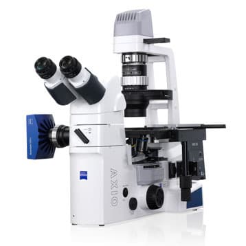
Carl Zeiss MicroscopyZEISS MERLIN Field Emission Scanning Electron Microscopes
Use the SEM/AFM (Atomic Force Microscopy) Hybrid option and get information on your semiconductor and nano materials samples at atomic resolution. Map large samples areas for design verification of semiconductor structures with the ATLAS large area mapping module. Explore non-conducting samples such as minerals, ceramics, glass and polymers with no compromises in beam voltage, detection and analytics due to the charge compensation by localized variable pressure.
Conveniently comprehend the topography and surface roughness of MEMS devices, nano structures, indentations for hardness measurements, or scratch marks in forensic investigations with real time 3DSM imaging module. The unique lens design image magnetic samples with no image distortions.
The ZEISS MERLIN complete detection system with the energy selective backscattered (EsB) on axis detection is ideally suited to reveal compositional details in nanocomposits, polymers, high strength steels and semiconductor structures.
Prices direct from Carl Zeiss Microscopy
Quick response times
Exclusive Labsave savings/discounts
Latest promotions
<p>Currently, we offer a great package deal for our tube handling systems. When you buy a HT500 or HT700 tube sorting system, you will receive a sample storage essentials pack for free. This comprises a single tube reader (DT510) and a rack reader (DR900), as well as a free case of tubes of your choice. This package will allow you to get started with efficient and high quality sample sorting.</p>
Avoid the risks associated with sample transfer and reduce hands-on time when you bind, wash, elute and/or concentrate your protein in the all-in-one...
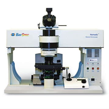
BaySpec, Inc. is offering special academic discount with the new NomadicTM multi-excitation confocal Raman microscope. NomadicTM is the only Raman microscope...
15% off on BMT Incubators - Climacell, Friocell, Incucell / Incucell V. On-Line Special 15% Discount on all Incubators, including Incubator options. •...
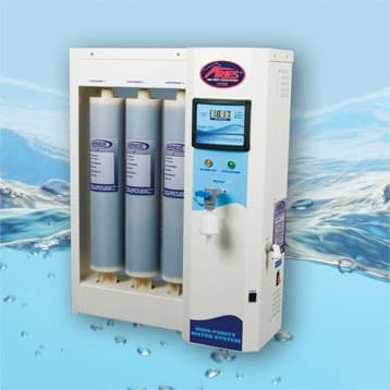
Order any Aries FilterWorks High Purity Lab Water Purification System an receive the first Years’ worth of Carbon and/or DI filters free! Please...
Combination Really-Flow™ Fluoride electrode, Epoxy body, Single Junction, Refillable with 1 meter low-noise cable and BNC connector. Weiss...
Jenway’s 73 series spectrophotometer range provides four models with a narrow spectral bandwidth of 5nm and an absorbance range of –0.3 to 2.5A,...
Top suppliers
NuAire, Inc.
63 products
PCE Instruments UK Ltd
19 products
Randox Laboratories
189 products
Panasonic Healthcare Company
5 products
Life Technologies
1 products
Nikon Instruments Europe
11 products
Olympus Europa Holding GmbH
3 products
GE Healthcare Life Sciences
2 products
Tecan Trading AG
19 products
BD (Becton, Dickinson and Company)
KEYENCE Corporation
5 products
RANDOX TOXICOLOGY
5 products
Randox Food Diagnostics
6 products

.jpg&w=640&q=75)

.jpg&w=640&q=75)

.jpg&w=640&q=75)


